Shanghai, September 12, 2025 — An international research collaboration led by East China University of Science and Technology (ECUST) has developed a novel method for fabricating advanced photoresist films, a critical material for next-generation semiconductor manufacturing. The work, published in Nature Chemical Engineering, demonstrates a controllable process for creating amorphous Zeolitic Imidazolate Framework (aZIF) films for high-precision lithography.
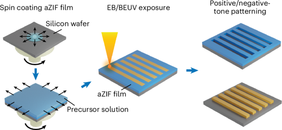
Facing the challenge of achieving large-area, uniform coating of photoresists on wafers, the team proposed an intermittent spin-coating chemical liquid deposition method. This technique allows precise control over the deposition rate and final thickness of aZIF films, ranging from a few nanometers to several hundred nanometers.
To optimize the process, researchers combined experiments with a 3D-printed micro-stirred continuous flow reactor and computational fluid dynamics simulations. This integrated approach helped identify the key factors affecting deposition uniformity. The team successfully fabricated various aZIF films, which were then tested as both positive and negative photoresists using electron beam lithography. Crucially, the films also demonstrated promising performance in beyond extreme ultraviolet lithography (Beyond EUVL) tests at wavelengths around 6.5–6.7 nm.
This research, involving collaborators from Johns Hopkins University and U.S. national laboratories, represents a significant step toward scalable and precise photoresist fabrication for future semiconductor devices.